Lessons In Electric Circuits -- Volume III (Semiconductors) - Chapter 3
Previous Contents
 Next
Next
Lessons In Electric Circuits -- Volume III
Chapter 3
DIODES AND RECTIFIERS
- Introduction
- Meter check of a diode
- Diode ratings
- Rectifier circuits
- Clipper circuits
- Clamper circuits
- Voltage multipliers
- Inductor commutating circuits
- Zener diodes
- Special-purpose diodes
- Other diode technologies
- Contributors
*** INCOMPLETE ***
Introduction
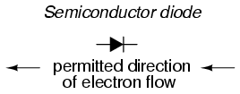
A diode is an electrical device allowing current to move through it in one direction with far greater ease than in the other. The most common type of diode in modern circuit design is the semiconductor diode, although other diode technologies exist. Semiconductor diodes are symbolized in schematic diagrams as such:
When placed in a simple battery-lamp circuit, the diode will either allow or prevent current through the lamp, depending on the polarity of the applied voltage:
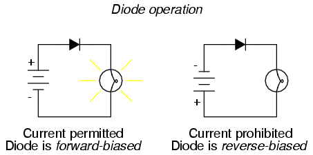
When the polarity of the battery is such that electrons are allowed to flow through the diode, the diode is said to be forward-biased. Conversely, when the battery is "backward" and the diode blocks current, the diode is said to be reverse-biased. A diode may be thought of as a kind of switch: "closed" when forward-biased and "open" when reverse-biased.
Oddly enough, the direction of the diode symbol's "arrowhead" points against the direction of electron flow. This is because the diode symbol was invented by engineers, who predominantly use conventional flow notation in their schematics, showing current as a flow of charge from the positive (+) side of the voltage source to the negative (-). This convention holds true for all semiconductor symbols possessing "arrowheads:" the arrow points in the permitted direction of conventional flow, and against the permitted direction of electron flow.
Diode behavior is analogous to the behavior of a hydraulic device called a check valve. A check valve allows fluid flow through it in one direction only:
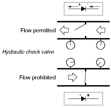
Check valves are essentially pressure-operated devices: they open and allow flow if the pressure across them is of the correct "polarity" to open the gate (in the analogy shown, greater fluid pressure on the right than on the left). If the pressure is of the opposite "polarity," the pressure difference across the check valve will close and hold the gate so that no flow occurs.
Like check valves, diodes are essentially "pressure-" operated (voltage-operated) devices. The essential difference between forward-bias and reverse-bias is the polarity of the voltage dropped across the diode. Let's take a closer look at the simple battery-diode-lamp circuit shown earlier, this time investigating voltage drops across the various components:
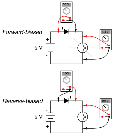
When the diode is forward-biased and conducting current, there is a small voltage dropped across it, leaving most of the battery voltage dropped across the lamp. When the battery's polarity is reversed and the diode becomes reverse-biased, it drops all of the battery's voltage and leaves none for the lamp. If we consider the diode to be a sort of self-actuating switch (closed in the forward-bias mode and open in the reverse-bias mode), this behavior makes sense. The most substantial difference here is that the diode drops a lot more voltage when conducting than the average mechanical switch (0.7 volts versus tens of millivolts).
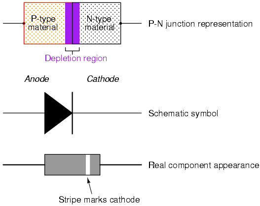
This forward-bias voltage drop exhibited by the diode is due to the action of the depletion region formed by the P-N junction under the influence of an applied voltage. When there is no voltage applied across a semiconductor diode, a thin depletion region exists around the region of the P-N junction, preventing current through it. The depletion region is for the most part devoid of available charge carriers and so acts as an insulator:
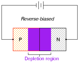
If a reverse-biasing voltage is applied across the P-N junction, this depletion region expands, further resisting any current through it:
Conversely, if a forward-biasing voltage is applied across the P-N junction, the depletion region will collapse and become thinner, so that the diode becomes less resistive to current through it. In order for a sustained current to go through the diode, though, the depletion region must be fully collapsed by the applied voltage. This takes a certain minimum voltage to accomplish, called the forward voltage:
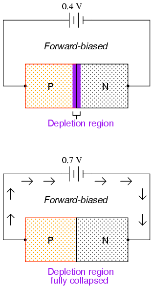
For silicon diodes, the typical forward voltage is 0.7 volts, nominal. For germanium diodes, the forward voltage is only 0.3 volts. The chemical constituency of the P-N junction comprising the diode accounts for its nominal forward voltage figure, which is why silicon and germanium diodes have such different forward voltages. Forward voltage drop remains approximately equal for a wide range of diode currents, meaning that diode voltage drop not like that of a resistor or even a normal (closed) switch. For most purposes of circuit analysis, it may be assumed that the voltage drop across a conducting diode remains constant at the nominal figure and is not related to the amount of current going through it.
In actuality, things are more complex than this. There is an equation describing the exact current through a diode, given the voltage dropped across the junction, the temperature of the junction, and several physical constants. It is commonly known as the diode equation:
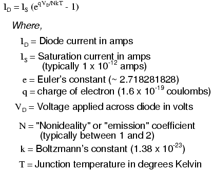
The equation kT/q describes the voltage produced within the P-N junction due to the action of temperature, and is called the thermal voltage, or Vt of the junction. At room temperature, this is about 26 millivolts. Knowing this, and assuming a "nonideality" coefficient of 1, we may simplify the diode equation and re-write it as such:
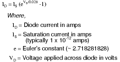
You need not be familiar with the "diode equation" in order to analyze simple diode circuits. Just understand that the voltage dropped across a current-conducting diode does change with the amount of current going through it, but that this change is fairly small over a wide range of currents. This is why many textbooks simply say the voltage drop across a conducting, semiconductor diode remains constant at 0.7 volts for silicon and 0.3 volts for germanium. However, some circuits intentionally make use of the P-N junction's inherent exponential current/voltage relationship and thus can only be understood in the context of this equation. Also, since temperature is a factor in the diode equation, a forward-biased P-N junction may also be used as a temperature-sensing device, and thus can only be understood if one has a conceptual grasp on this mathematical relationship.
A reverse-biased diode prevents current from going through it, due to the expanded depletion region. In actuality, a very small amount of current can and does go through a reverse-biased diode, called the leakage current, but it can be ignored for most purposes. The ability of a diode to withstand reverse-bias voltages is limited, like it is for any insulating substance or device. If the applied reverse-bias voltage becomes too great, the diode will experience a condition known as breakdown, which is usually destructive. A diode's maximum reverse-bias voltage rating is known as the Peak Inverse Voltage, or PIV, and may be obtained from the manufacturer. Like forward voltage, the PIV rating of a diode varies with temperature, except that PIV increases with increased temperature and decreases as the diode becomes cooler -- exactly opposite that of forward voltage.
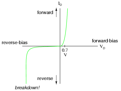
Typically, the PIV rating of a generic "rectifier" diode is at least 50 volts at room temperature. Diodes with PIV ratings in the many thousands of volts are available for modest prices.
- REVIEW:
- A diode is an electrical component acting as a one-way valve for current.
- When voltage is applied across a diode in such a way that the diode allows current, the diode is said to be forward-biased.
- When voltage is applied across a diode in such a way that the diode prohibits current, the diode is said to be reverse-biased.
- The voltage dropped across a conducting, forward-biased diode is called the forward voltage. Forward voltage for a diode varies only slightly for changes in forward current and temperature, and is fixed principally by the chemical composition of the P-N junction.
- Silicon diodes have a forward voltage of approximately 0.7 volts.
- Germanium diodes have a forward voltage of approximately 0.3 volts.
- The maximum reverse-bias voltage that a diode can withstand without "breaking down" is called the Peak Inverse Voltage, or PIV rating.
Meter check of a diode
Being able to determine the polarity (cathode versus anode) and basic functionality of a diode is a very important skill for the electronics hobbyist or technician to have. Since we know that a diode is essentially nothing more than a one-way valve for electricity, it makes sense we should be able to verify its one-way nature using a DC (battery-powered) ohmmeter. Connected one way across the diode, the meter should show a very low resistance. Connected the other way across the diode, it should show a very high resistance ("OL" on some digital meter models):
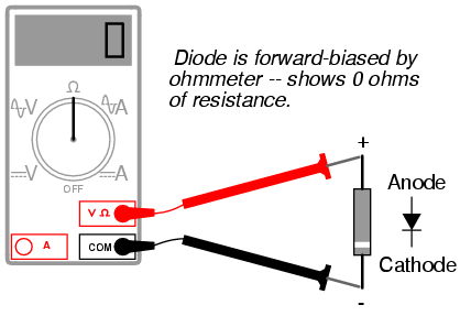
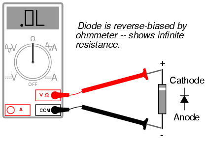
Of course, in order to determine which end of the diode is the cathode and which is the anode, you must know with certainty which test lead of the meter is positive (+) and which is negative (-) when set to the "resistance" or "Ω" function. With most digital multimeters I've seen, the red lead becomes positive and the black lead negative when set to measure resistance, in accordance with standard electronics color-code convention. However, this is not guaranteed for all meters. Many analog multimeters, for example, actually make their black leads positive (+) and their red leads negative (-) when switched to the "resistance" function, because it is easier to manufacture it that way!
One problem with using an ohmmeter to check a diode is that the readings obtained only have qualitative value, not quantitative. In other words, an ohmmeter only tells you which way the diode conducts; the low-value resistance indication obtained while conducting is useless. If an ohmmeter shows a value of "1.73 ohms" while forward-biasing a diode, that figure of 1.73 Ω doesn't represent any real-world quantity useful to us as technicians or circuit designers. It neither represents the forward voltage drop nor any "bulk" resistance in the semiconductor material of the diode itself, but rather is a figure dependent upon both quantities and will vary substantially with the particular ohmmeter used to take the reading.
For this reason, some digital multimeter manufacturers equip their meters with a special "diode check" function which displays the actual forward voltage drop of the diode in volts, rather than a "resistance" figure in ohms. These meters work by forcing a small current through the diode and measuring the voltage dropped between the two test leads:
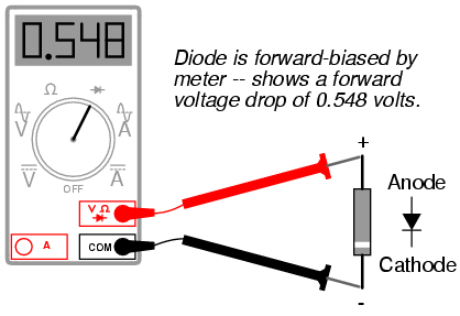
The forward voltage reading obtained with such a meter will typically be less than the "normal" drop of 0.7 volts for silicon and 0.3 volts for germanium, because the current provided by the meter is of trivial proportions. If a multimeter with diode-check function isn't available, or you would like to measure a diode's forward voltage drop at some non-trivial current, the following circuit may be constructed using nothing but a battery, resistor, and a normal voltmeter:
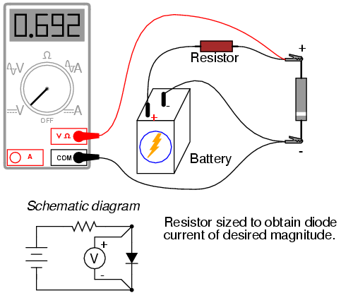
Connecting the diode backwards to this testing circuit will simply result in the voltmeter indicating the full voltage of the battery.
If this circuit were designed so as to provide a constant or nearly constant current through the diode despite changes in forward voltage drop, it could be used as the basis of a temperature-measurement instrument, the voltage measured across the diode being inversely proportional to diode junction temperature. Of course, diode current should be kept to a minimum to avoid self-heating (the diode dissipating substantial amounts of heat energy), which would interfere with temperature measurement.
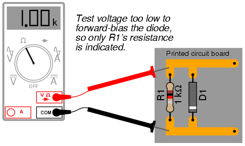
Beware that some digital multimeters equipped with a "diode check" function may output a very low test voltage (less than 0.3 volts) when set to the regular "resistance" (Ω) function: too low to fully collapse the depletion region of a PN junction. The philosophy here is that the "diode check" function is to be used for testing semiconductor devices, and the "resistance" function for anything else. By using a very low test voltage to measure resistance, it is easier for a technician to measure the resistance of non-semiconductor components connected to semiconductor components, since the semiconductor component junctions will not become forward-biased with such low voltages.
Consider the example of a resistor and diode connected in parallel, soldered in place on a printed circuit board (PCB). Normally, one would have to unsolder the resistor from the circuit (disconnect it from all other components) before being able to measure its resistance, otherwise any parallel-connected components would affect the reading obtained. However, using a multimeter that outputs a very low test voltage to the probes in the "resistance" function mode, the diode's PN junction will not have enough voltage impressed across it to become forward-biased, and as such will pass negligible current. Consequently, the meter "sees" the diode as an open (no continuity), and only registers the resistor's resistance:
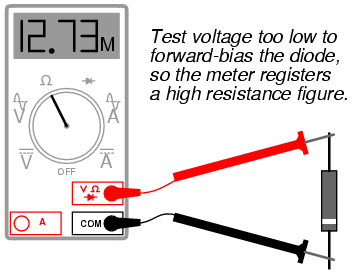
If such an ohmmeter were used to test a diode, it would indicate a very high resistance (many mega-ohms) even if connected to the diode in the "correct" (forward-biased) direction:
Reverse voltage strength of a diode is not as easily tested, because exceeding a normal diode's PIV usually results in destruction of the diode. There are special types of diodes, though, which are designed to "break down" in reverse-bias mode without damage (called Zener diodes), and they are best tested with the same type of voltage source / resistor / voltmeter circuit, provided that the voltage source is of high enough value to force the diode into its breakdown region. More on this subject in a later section of this chapter.
- REVIEW:
- An ohmmeter may be used to qualitatively check diode function. There should be low resistance measured one way and very high resistance measured the other way. When using an ohmmeter for this purpose, be sure you know which test lead is positive and which is negative! The actual polarity may not follow the colors of the leads as you might expect, depending on the particular design of meter.
- Some multimeters provide a "diode check" function that displays the actual forward voltage of the diode when it's conducting current. Such meters typically indicate a slightly lower forward voltage than what is "nominal" for a diode, due to the very small amount of current used during the check.
Diode ratings
In addition to forward voltage drop (Vf) and peak inverse voltage (PIV), there are many other ratings of diodes important to circuit design and component selection. Semiconductor manufacturers provide detailed specifications on their products -- diodes included -- in publications known as datasheets. Datasheets for a wide variety of semiconductor components may be found in reference books and on the internet. I personally prefer the internet as a source of component specifications because all the data obtained from manufacturer websites are up-to-date.
A typical diode datasheet will contain figures for the following parameters:
Maximum repetitive reverse voltage = VRRM, the maximum amount of voltage the diode can withstand in reverse-bias mode, in repeated pulses. Ideally, this figure would be infinite.
Maximum DC reverse voltage = VR or VDC, the maximum amount of voltage the diode can withstand in reverse-bias mode on a continual basis. Ideally, this figure would be infinite.
Maximum forward voltage = VF, usually specified at the diode's rated forward current. Ideally, this figure would be zero: the diode providing no opposition whatsoever to forward current. In reality, the forward voltage is described by the "diode equation."
Maximum (average) forward current = IF(AV), the maximum average amount of current the diode is able to conduct in forward bias mode. This is fundamentally a thermal limitation: how much heat can the PN junction handle, given that dissipation power is equal to current (I) multiplied by voltage (V or E) and forward voltage is dependent upon both current and junction temperature. Ideally, this figure would be infinite.
Maximum (peak or surge) forward current = IFSM or if(surge), the maximum peak amount of current the diode is able to conduct in forward bias mode. Again, this rating is limited by the diode junction's thermal capacity, and is usually much higher than the average current rating due to thermal inertia (the fact that it takes a finite amount of time for the diode to reach maximum temperature for a given current). Ideally, this figure would be infinite.
Maximum total dissipation = PD, the amount of power (in watts) allowable for the diode to dissipate, given the dissipation (P=IE) of diode current multiplied by diode voltage drop, and also the dissipation (P=I2R) of diode current squared multiplied by bulk resistance. Fundamentally limited by the diode's thermal capacity (ability to tolerate high temperatures).
Operating junction temperature = TJ, the maximum allowable temperature for the diode's PN junction, usually given in degrees Celsius (oC). Heat is the "Achilles' heel" of semiconductor devices: they must be kept cool to function properly and give long service life.
Storage temperature range = TSTG, the range of allowable temperatures for storing a diode (unpowered). Sometimes given in conjunction with operating junction temperature (TJ), because the maximum storage temperature and the maximum operating temperature ratings are often identical. If anything, though, maximum storage temperature rating will be greater than the maximum operating temperature rating.
Thermal resistance = R(Θ), the temperature difference between junction and outside air (R(Θ)JA) or between junction and leads (R(Θ)JL) for a given power dissipation. Expressed in units of degrees Celsius per watt (oC/W). Ideally, this figure would be zero, meaning that the diode package was a perfect thermal conductor and radiator, able to transfer all heat energy from the junction to the outside air (or to the leads) with no difference in temperature across the thickness of the diode package. A high thermal resistance means that the diode will build up excessive temperature at the junction (where it's critical) despite best efforts at cooling the outside of the diode, and thus will limit its maximum power dissipation.
Maximum reverse current = IR, the amount of current through the diode in reverse-bias operation, with the maximum rated inverse voltage applied (VDC). Sometimes referred to as leakage current. Ideally, this figure would be zero, as a perfect diode would block all current when reverse-biased. In reality, it is very small compared to the maximum forward current.
Typical junction capacitance = CJ, the typical amount of capacitance intrinsic to the junction, due to the depletion region acting as a dielectric separating the anode and cathode connections. This is usually a very small figure, measured in the range of picofarads (pF).
Reverse recovery time = trr, the amount of time it takes for a diode to "turn off" when the voltage across it alternates from forward-bias to reverse-bias polarity. Ideally, this figure would be zero: the diode halting conduction immediately upon polarity reversal. For a typical rectifier diode, reverse recovery time is in the range of tens of microseconds; for a "fast switching" diode, it may only be a few nanoseconds.
Most of these parameters vary with temperature or other operating conditions, and so a single figure fails to fully describe any given rating. Therefore, manufacturers provide graphs of component ratings plotted against other variables (such as temperature), so that the circuit designer has a better idea of what the device is capable of.
Rectifier circuits
Now we come to the most popular application of the diode: rectification. Simply defined, rectification is the conversion of alternating current (AC) to direct current (DC). This almost always involves the use of some device that only allows one-way flow of electrons. As we have seen, this is exactly what a semiconductor diode does. The simplest type of rectifier circuit is the half-wave rectifier, so called because it only allows one half of an AC waveform to pass through to the load:
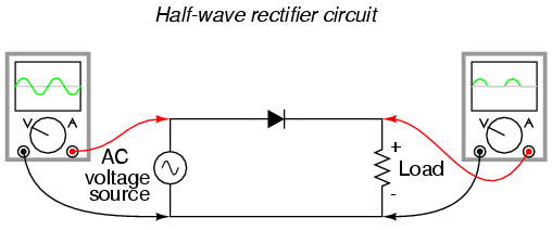
For most power applications, half-wave rectification is insufficient for the task. The harmonic content of the rectifier's output waveform is very large and consequently difficult to filter. Furthermore, AC power source only works to supply power to the load once every half-cycle, meaning that much of its capacity is unused. Half-wave rectification is, however, a very simple way to reduce power to a resistive load. Some two-position lamp dimmer switches apply full AC power to the lamp filament for "full" brightness and then half-wave rectify it for a lesser light output:
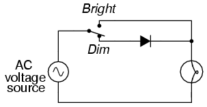
In the "Dim" switch position, the incandescent lamp receives approximately one-half the power it would normally receive operating on full-wave AC. Because the half-wave rectified power pulses far more rapidly than the filament has time to heat up and cool down, the lamp does not blink. Instead, its filament merely operates at a lesser temperature than normal, providing less light output. This principle of "pulsing" power rapidly to a slow-responding load device in order to control the electrical power sent to it is very common in the world of industrial electronics. Since the controlling device (the diode, in this case) is either fully conducting or fully nonconducting at any given time, it dissipates little heat energy while controlling load power, making this method of power control very energy-efficient. This circuit is perhaps the crudest possible method of pulsing power to a load, but it suffices as a proof-of-concept application.
If we need to rectify AC power so as to obtain the full use of both half-cycles of the sine wave, a different rectifier circuit configuration must be used. Such a circuit is called a full-wave rectifier. One type of full-wave rectifier, called the center-tap design, uses a transformer with a center-tapped secondary winding and two diodes, like this:
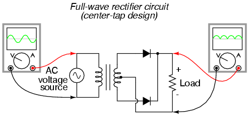
This circuit's operation is easily understood one half-cycle at a time. Consider the first half-cycle, when the source voltage polarity is positive (+) on top and negative (-) on bottom. At this time, only the top diode is conducting; the bottom diode is blocking current, and the load "sees" the first half of the sine wave, positive on top and negative on bottom. Only the top half of the transformer's secondary winding carries current during this half-cycle:
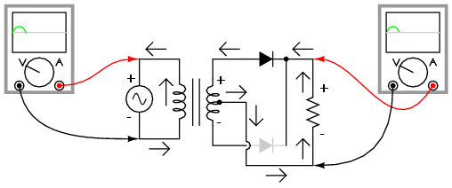
During the next half-cycle, the AC polarity reverses. Now, the other diode and the other half of the transformer's secondary winding carry current while the portions of the circuit formerly carrying current during the last half-cycle sit idle. The load still "sees" half of a sine wave, of the same polarity as before: positive on top and negative on bottom:
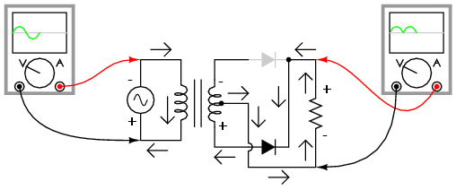
One disadvantage of this full-wave rectifier design is the necessity of a transformer with a center-tapped secondary winding. If the circuit in question is one of high power, the size and expense of a suitable transformer is significant. Consequently, the center-tap rectifier design is seen only in low-power applications.
Another, more popular full-wave rectifier design exists, and it is built around a four-diode bridge configuration. For obvious reasons, this design is called a full-wave bridge:
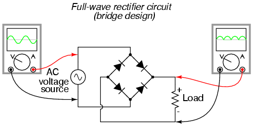
Current directions in the full-wave bridge rectifier circuit are as follows for each half-cycle of the AC waveform:
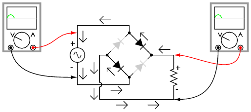
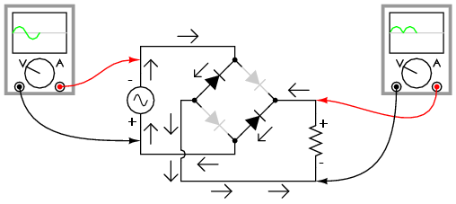
Remembering the proper layout of diodes in a full-wave bridge rectifier circuit can often be frustrating to the new student of electronics. I've found that an alternative representation of this circuit is easier both to remember and to comprehend. It's the exact same circuit, except all diodes are drawn in a horizontal attitude, all "pointing" the same direction:
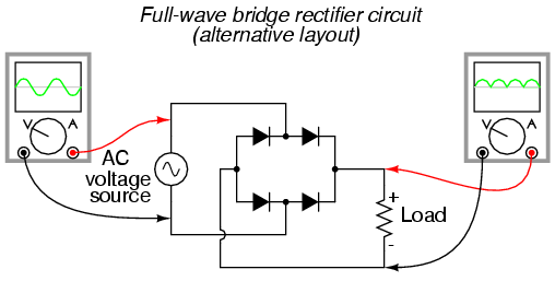
One advantage of remembering this layout for a bridge rectifier circuit is that it expands easily into a polyphase version:
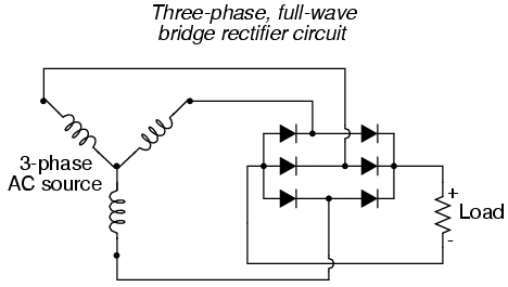
Each three-phase line connects between a pair of diodes: one to route power to the positive (+) side of the load, and the other to route power to the negative (-) side of the load. Polyphase systems with more than three phases are easily accommodated into a bridge rectifier scheme. Take for instance this six-phase bridge rectifier circuit:
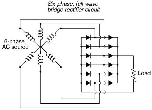
When polyphase AC is rectified, the phase-shifted pulses overlap each other to produce a DC output that is much "smoother" (has less AC content) than that produced by the rectification of single-phase AC. This is a decided advantage in high-power rectifier circuits, where the sheer physical size of filtering components would be prohibitive but low-noise DC power must be obtained. The following diagram shows the full-wave rectification of three-phase AC:
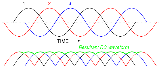
In any case of rectification -- single-phase or polyphase -- the amount of AC voltage mixed with the rectifier's DC output is called ripple voltage. In most cases, since "pure" DC is the desired goal, ripple voltage is undesirable. If the power levels are not too great, filtering networks may be employed to reduce the amount of ripple in the output voltage.
Sometimes, the method of rectification is referred to by counting the number of DC "pulses" output for every 360o of electrical "rotation." A single-phase, half-wave rectifier circuit, then, would be called a 1-pulse rectifier, because it produces a single pulse during the time of one complete cycle (360o) of the AC waveform. A single-phase, full-wave rectifier (regardless of design, center-tap or bridge) would be called a 2-pulse rectifier, because it outputs two pulses of DC during one AC cycle's worth of time. A three-phase full-wave rectifier would be called a 6-pulse unit.
Modern electrical engineering convention further describes the function of a rectifier circuit by using a three-field notation of phases, ways, and number of pulses. A single-phase, half-wave rectifier circuit is given the somewhat cryptic designation of 1Ph1W1P (1 phase, 1 way, 1 pulse), meaning that the AC supply voltage is single-phase, that current on each phase of the AC supply lines moves in one direction (way) only, and that there is a single pulse of DC produced for every 360o of electrical rotation. A single-phase, full-wave, center-tap rectifier circuit would be designated as 1Ph1W2P in this notational system: 1 phase, 1 way or direction of current in each winding half, and 2 pulses or output voltage per cycle. A single-phase, full-wave, bridge rectifier would be designated as 1Ph2W2P: the same as for the center-tap design, except current can go both ways through the AC lines instead of just one way. The three-phase bridge rectifier circuit shown earlier would be called a 3Ph2W6P rectifier.
Is it possible to obtain more pulses than twice the number of phases in a rectifier circuit? The answer to this question is yes: especially in polyphase circuits. Through the creative use of transformers, sets of full-wave rectifiers may be paralleled in such a way that more than six pulses of DC are produced for three phases of AC. A 30o phase shift is introduced from primary to secondary of a three-phase transformer when the winding configurations are not of the same type. In other words, a transformer connected either Y-Δ or Δ-Y will exhibit this 30o phase shift, while a transformer connected Y-Y or Δ-Δ will not. This phenomenon may be exploited by having one transformer connected Y-Y feed a bridge rectifier, and have another transformer connected Y-Δ feed a second bridge rectifier, then parallel the DC outputs of both rectifiers. Since the ripple voltage waveforms of the two rectifiers' outputs are phase-shifted 30o from one another, their superposition results in less ripple than either rectifier output considered separately: 12 pulses per 360o instead of just six:
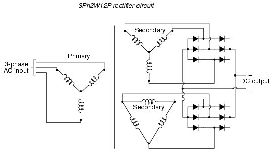
- REVIEW:
- Rectification is the conversion of alternating current (AC) to direct current (DC).
- A half-wave rectifier is a circuit that allows only one half-cycle of the AC voltage waveform to be applied to the load, resulting in one non-alternating polarity across it. The resulting DC delivered to the load "pulsates" significantly.
- A full-wave rectifier is a circuit that converts both half-cycles of the AC voltage waveform to an unbroken series of voltage pulses of the same polarity. The resulting DC delivered to the load doesn't "pulsate" as much.
- Polyphase alternating current, when rectified, gives a much "smoother" DC waveform (less ripple voltage) than rectified single-phase AC.
Clipper circuits
Clamper circuits
Voltage multipliers
Inductor commutating circuits
A popular use of diodes is for the mitigation of inductive "kickback:" the pulses of high voltage produced when direct current through an inductor is interrupted. Take for example this simple circuit:
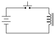
When the pushbutton switch is actuated, current goes through the inductor, producing a magnetic field around it. When the switch is de-actuated, its contacts open, interrupting current through the inductor, and causing the magnetic field to rapidly collapse. Because the voltage induced in a coil of wire is directly proportional to the rate of change over time of magnetic flux (Faraday's Law: e = NdΦ/dt), this rapid collapse of magnetism around the coil produces a high voltage "spike."
If the inductor in question is an electromagnet coil, such as might be seen in a solenoid or relay (constructed for the purpose of creating a physical force via its magnetic field when energized), the effect of inductive "kickback" serves no useful purpose at all. In fact, it is quite detrimental to the switch, as it will cause excessive arcing at the contacts, greatly reducing their service life. There are several practical methods of mitigating the high voltage transient created when the switch is opened, but none so simple as the so-called commutating diode:
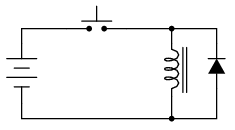
In this circuit, the diode is placed in parallel with the coil, in such a way that it will be reverse-biased when DC voltage is applied to the coil through the switch. Thus, when the coil is energized, the diode conducts no current:
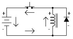
However, when the switch is opened, the coil's inductance responds to the decrease in current by inducing a voltage of reverse polarity, in an effort to maintain current at the same magnitude and in the same direction. This sudden reversal of voltage polarity across the coil forward-biases the diode, and the diode provides a current path for the inductor's current, so that its stored energy is dissipated slowly rather than suddenly:
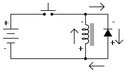
As a result, the voltage induced in the coil by its collapsing magnetic field is quite low: merely the forward voltage drop of the diode, rather than hundreds of volts as before. Thus, the switch contacts experience a voltage drop equal to the battery voltage plus about 0.7 volts (if the diode is silicon) during this discharge time.
In electronics parlance, commutation refers to the reversal of voltage polarity or current direction. Thus, the purpose of a commutating diode is to act whenever voltage reverses polarity, in this case, the voltage induced by the inductor coil when current through it is interrupted by the switch. A less formal term for a commutating diode is snubber, because it "snubs" or "squelches" the inductive kickback.
A noteworthy disadvantage of this method is the extra time it imparts to the coil's discharge. Because the induced voltage is clamped to a very low value, its rate of magnetic flux change over time is comparatively slow. Remember that Faraday's Law describes the magnetic flux rate-of-change (dΦ/dt) as being proportional to the induced, instantaneous voltage (e or v). If the instantaneous voltage is limited to some low figure, then the rate of change of magnetic flux over time will likewise be limited to a low (slow) figure.
If an electromagnet coil is "snubbed" with a commutating diode, the magnetic field will dissipate at a relatively slow rate compared to the original scenario (no diode) where the field disappeared almost instantly upon switch release. The amount of time in question will most likely be less than one second, but it will be measurably slower than without a commutating diode in place. This may be an intolerable consequence if the coil is used to actuate an electromechanical relay, because the relay will possess a natural "time delay" upon coil de-energization, and an unwanted delay of even a fraction of a second may wreak havoc in some circuits.
Unfortunately, there is no way to eliminate the high-voltage transient of inductive kickback and maintain fast de-magnetization of the coil: Faraday's Law will not be violated. However, if slow de-magnetization is unacceptable, a compromise may be struck between transient voltage and time by allowing the coil's voltage to rise to some higher level (but not so high as without a commutating diode in place). The following schematic shows how this may be done:
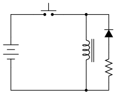
A resistor placed in series with the commutating diode allows the coil's induced voltage to rise to a level greater than the diode's forward voltage drop, thus hastening the process of de-magnetization. This, of course, will place the switch contacts under greater stress, and so the resistor must be sized to limit that transient voltage at an acceptable maximum level.
Zener diodes
If we connect a diode and resistor in series with a DC voltage source so that the diode is forward-biased, the voltage drop across the diode will remain fairly constant over a wide range of power supply voltages:

According to the "diode equation," the current through a forward-biased PN junction is proportional to e raised to the power of the forward voltage drop. Because this is an exponential function, current rises quite rapidly for modest increases in voltage drop. Another way of considering this is to say that voltage dropped across a forward-biased diode changes little for large variations in diode current. In the circuit shown above, diode current is limited by the voltage of the power supply, the series resistor, and the diode's voltage drop, which as we know doesn't vary much from 0.7 volts. If the power supply voltage were to be increased, the resistor's voltage drop would increase almost the same amount, and the diode's voltage drop just a little. Conversely, a decrease in power supply voltage would result in an almost equal decrease in resistor voltage drop, with just a little decrease in diode voltage drop. In a word, we could summarize this behavior by saying that the diode is regulating the voltage drop at approximately 0.7 volts.
Voltage regulation is a useful diode property to exploit. Suppose we were building some kind of circuit which could not tolerate variations in power supply voltage, but needed to be powered by a chemical battery, whose voltage changes over its lifetime. We could form a circuit as shown and connect the circuit requiring steady voltage across the diode, where it would receive an unchanging 0.7 volts.
This would certainly work, but most practical circuits of any kind require a power supply voltage in excess of 0.7 volts to properly function. One way we could increase our voltage regulation point would be to connect multiple diodes in series, so that their individual forward voltage drops of 0.7 volts each would add to create a larger total. For instance, if we had ten diodes in series, the regulated voltage would be ten times 0.7, or 7 volts:
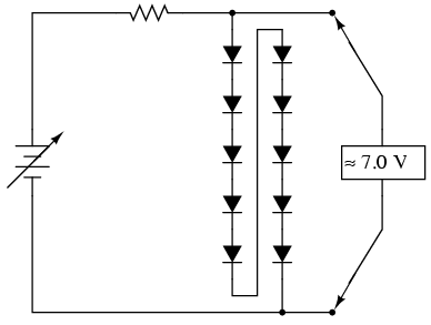
So long as the battery voltage never sagged below 7 volts, there would always be about 7 volts dropped across the ten-diode "stack."
If larger regulated voltages are required, we could either use more diodes in series (an inelegant option, in my opinion), or try a fundamentally different approach. We know that diode forward voltage is a fairly constant figure under a wide range of conditions, but so is reverse breakdown voltage, and breakdown voltage is typically much, much greater than forward voltage. If we reversed the polarity of the diode in our single-diode regulator circuit and increased the power supply voltage to the point where the diode "broke down" (could no longer withstand the reverse-bias voltage impressed across it), the diode would similarly regulate the voltage at that breakdown point, not allowing it to increase further:
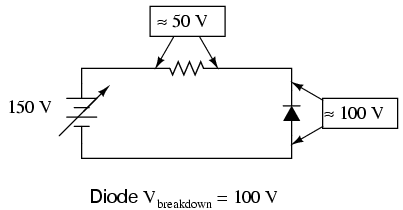
Unfortunately, when normal rectifying diodes "break down," they usually do so destructively. However, it is possible to build a special type of diode that can handle breakdown without failing completely. This type of diode is called a zener diode, and its symbol looks like this:
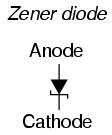
When forward-biased, zener diodes behave much the same as standard rectifying diodes: they have a forward voltage drop which follows the "diode equation" and is about 0.7 volts. In reverse-bias mode, they do not conduct until the applied voltage reaches or exceeds the so-called zener voltage, at which point the diode is able to conduct substantial current, and in doing so will try to limit the voltage dropped across it to that zener voltage point. So long as the power dissipated by this reverse current does not exceed the diode's thermal limits, the diode will not be harmed.
Zener diodes are manufactured with zener voltages ranging anywhere from a few volts to hundreds of volts. This zener voltage changes slightly with temperature, and like common carbon-composition resistor values, may be anywhere from 5 percent to 10 percent in error from the manufacturer's specifications. However, this stability and accuracy is generally good enough for the zener diode to be used as a voltage regulator device in common power supply circuit:
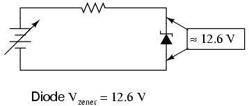
Please take note of the zener diode's orientation in the above circuit: the diode is reverse-biased, and intentionally so. If we had oriented the diode in the "normal" way, so as to be forward-biased, it would only drop 0.7 volts, just like a regular rectifying diode. If we want to exploit this diode's reverse breakdown properties, we must operate it in its reverse-bias mode. So long as the power supply voltage remains above the zener voltage (12.6 volts, in this example), the voltage dropped across the zener diode will remain at approximately 12.6 volts.
Like any semiconductor device, the zener diode is sensitive to temperature. Excessive temperature will destroy a zener diode, and because it both drops voltage and conducts current, it produces its own heat in accordance with Joule's Law (P=IE). Therefore, one must be careful to design the regulator circuit in such a way that the diode's power dissipation rating is not exceeded. Interestingly enough, when zener diodes fail due to excessive power dissipation, they usually fail shorted rather than open. A diode failed in this manner is easy to detect: it drops almost zero voltage when biased either way, like a piece of wire.
Let's examine a zener diode regulating circuit mathematically, determining all voltages, currents, and power dissipations. Taking the same form of circuit shown earlier, we'll perform calculations assuming a zener voltage of 12.6 volts, a power supply voltage of 45 volts, and a series resistor value of 1000 Ω (we'll regard the zener voltage to be exactly 12.6 volts so as to avoid having to qualify all figures as "approximate"):
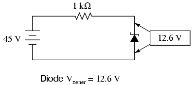
If the zener diode's voltage is 12.6 volts and the power supply's voltage is 45 volts, there will be 32.4 volts dropped across the resistor (45 volts - 12.6 volts = 32.4 volts). 32.4 volts dropped across 1000 Ω gives 32.4 mA of current in the circuit:
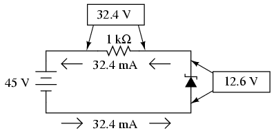
Power is calculated by multiplying current by voltage (P=IE), so we can calculate power dissipations for both the resistor and the zener diode quite easily:
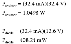
A zener diode with a power rating of 0.5 watt would be adequate, as would a resistor rated for 1.5 or 2 watts of dissipation.
If excessive power dissipation is detrimental, then why not design the circuit for the least amount of dissipation possible? Why not just size the resistor for a very high value of resistance, thus severely limiting current and keeping power dissipation figures very low? Take this circuit, for example, with a 100 kΩ resistor instead of a 1 kΩ resistor. Note that both the power supply voltage and the diode's zener voltage are identical to the last example:
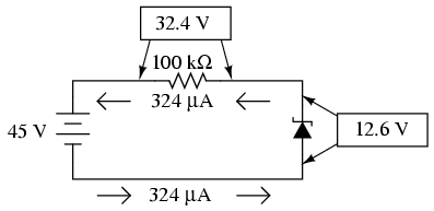
With only 1/100 of the current we had before (324 µA instead of 32.4 mA), both power dissipation figures should be 100 times smaller:
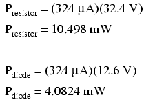
Seems ideal, doesn't it? Less power dissipation means lower operating temperatures for both the diode and the resistor, and also less wasted energy in the system, right? A higher resistance value does reduce power dissipation levels in the circuit, but it unfortunately introduces another problem. Remember that the purpose of a regulator circuit is to provide a stable voltage for another circuit. In other words, we're eventually going to power something with 12.6 volts, and this something will have a current draw of its own. Consider our first regulator circuit, this time with a 500 Ω load connected in parallel with the zener diode:
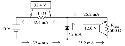
If 12.6 volts is maintained across a 500 Ω load, the load will draw 25.2 mA of current. In order for the 1 kΩ series "dropping" resistor to drop 32.4 volts (reducing the power supply's voltage of 45 volts down to 12.6 across the zener), it still must conduct 32.4 mA of current. This leaves 7.2 mA of current through the zener diode.
Now consider our "power-saving" regulator circuit with the 100 kΩ dropping resistor, delivering power to the same 500 Ω load. What it is supposed to do is maintain 12.6 volts across the load, just like the last circuit. However, as we will see, it cannot accomplish this task:
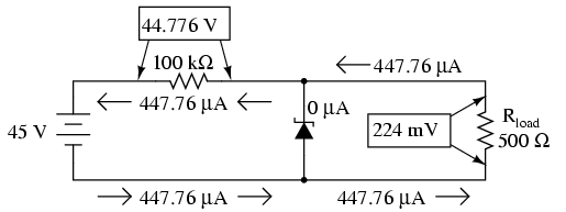
With the larger value of dropping resistor in place, there will only be about 224 mV of voltage across the 500 Ω load, far less than the expected value of 12.6 volts! Why is this? If we actually had 12.6 volts across the load, it would draw 25.2 mA of current, as before. This load current would have to go through the series dropping resistor as it did before, but with a new (much larger!) dropping resistor in place, the voltage dropped across that resistor with 25.2 mA of current going through it would be 2,520 volts! Since we obviously don't have that much voltage supplied by the battery, this cannot happen.
The situation is easier to comprehend if we temporarily remove the zener diode from the circuit and analyze the behavior of the two resistors alone:
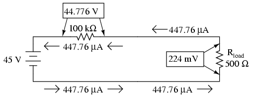
Both the 100 kΩ dropping resistor and the 500 Ω load resistance are in series with each other, giving a total circuit resistance of 100.5 kΩ. With a total voltage of 45 volts and a total resistance of 100.5 kΩ, Ohm's Law (I=E/R) tells us that the current will be 447.76 µA. Figuring voltage drops across both resistors (E=IR), we arrive at 44.776 volts and 224 mV, respectively. If we were to re-install the zener diode at this point, it would "see" 224 mV across it as well, being in parallel with the load resistance. This is far below the zener breakdown voltage of the diode and so it will not "break down" and conduct current. For that matter, at this low voltage the diode wouldn't conduct even if it were forward-biased! Thus, the diode ceases to regulate voltage, for it can do so only when there is at least 12.6 volts dropped across to "activate" it.
The analytical technique of removing a zener diode from a circuit and seeing whether or not there is enough voltage present to make it conduct is a sound one. Just because a zener diode happens to be connected in a circuit doesn't guarantee that the full zener voltage will always be dropped across it! Remember that zener diodes work by limiting voltage to some maximum level; they cannot make up for a lack of voltage.
In summary, any zener diode regulating circuit will function so long as the load's resistance is equal to or greater than some minimum value. If the load resistance is too low, it will draw too much current, dropping too much voltage across the series dropping resistor, leaving insufficient voltage across the zener diode to make it conduct. When the zener diode stops conducting current, it can no longer regulate voltage, and the load voltage will fall below the regulation point.
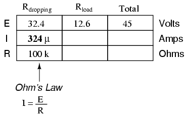
Our regulator circuit with the 100 kΩ dropping resistor must be good for some value of load resistance, though. To find this acceptable load resistance value, we can use a table to calculate resistance in the two-resistor series circuit (no diode), inserting the known values of total voltage and dropping resistor resistance, and calculating for an expected load voltage of 12.6 volts:
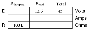
With 45 volts of total voltage and 12.6 volts across the load, we should have 32.4 volts across Rdropping:
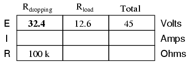
With 32.4 volts across the dropping resistor, and 100 kΩ worth of resistance in it, the current through it will be 324 µA:
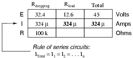
Being a series circuit, the current is equal through all components at any given time:
Calculating load resistance is now a simple matter of Ohm's Law (R = E/I), giving us 38.889 kΩ:
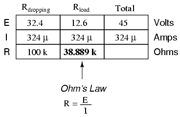
Thus, if the load resistance is exactly 38.889 kΩ, there will be 12.6 volts across it, diode or no diode. Any load resistance smaller than 38.889 kΩ will result in a load voltage less than 12.6 volts, diode or no diode. With the diode in place, the load voltage will be regulated to a maximum of 12.6 volts for any load resistance greater than 38.889 kΩ.
With the original value of 1 kΩ for the dropping resistor, our regulator circuit was able to adequately regulate voltage even for a load resistance as low as 500 Ω. What we see is a tradeoff between power dissipation and acceptable load resistance. The higher-value dropping resistor gave us less power dissipation, at the expense of raising the acceptable minimum load resistance value. If we wish to regulate voltage for low-value load resistances, the circuit must be prepared to handle higher power dissipation.
Zener diodes regulate voltage by acting as complementary loads, drawing more or less current as necessary to ensure a constant voltage drop across the load. This is analogous to regulating the speed of an automobile by braking rather than by varying the throttle position: not only is it wasteful, but the brakes must be built to handle all the engine's power when the driving conditions don't demand it. Despite this fundamental inefficiency of design, zener diode regulator circuits are widely employed due to their sheer simplicity. In high-power applications where the inefficiencies would be unacceptable, other voltage-regulating techniques are applied. But even then, small zener-based circuits are often used to provide a "reference" voltage to drive a more efficient amplifier-type of circuit controlling the main power.
- REVIEW:
- Zener diodes are designed to be operated in reverse-bias mode, providing a relatively low, stable breakdown, or zener voltage at which they being to conduct substantial reverse current.
- A zener diode may function as a voltage regulator by acting as an accessory load, drawing more current from the source if the voltage is too high, and less if it is too low.
Special-purpose diodes
Schottky diodes
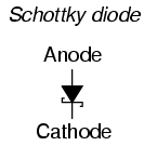
Schottky diodes are constructed of a metal-to-N junction rather than a P-N semiconductor junction. Also known as hot-carrier diodes, Schottky diodes are characterized by fast switching times (low reverse-recovery time), low forward voltage drop (typically 0.25 to 0.4 volts for a metal-silicon junction), and low junction capacitance.
The schematic symbol for a Schottky diode is shown here:
In terms of forward voltage drop (VF), reverse-recovery time (trr), and junction capacitance (CJ), Schottky diodes are closer to ideal than the average "rectifying" diode. This makes them well suited for high-frequency applications. Unfortunately, though, Schottky diodes typically have lower forward current (IF) and reverse voltage (VRRM and VDC) ratings than rectifying diodes and are thus unsuitable for applications involving substantial amounts of power.
Schottky diode technology finds broad application in high-speed computer circuits, where the fast switching time equates to high speed capability, and the low forward voltage drop equates to less power dissipation when conducting.
Tunnel diodes
Tunnel diodes exploit a strange quantum phenomenon called resonant tunneling to provide interesting forward-bias characteristics. When a small forward-bias voltage is applied across a tunnel diode, it begins to conduct current. As the voltage is increased, the current increases and reaches a peak value called the peak current (IP). If the voltage is increased a little more, the current actually begins to decrease until it reaches a low point called the valley current (IV). If the voltage is increased further yet, the current begins to increase again, this time without decreasing into another "valley." Both the schematic symbol and a current/voltage plot for the tunnel diode are shown in the following illustration:
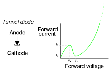
The forward voltages necessary to drive a tunnel diode to its peak and valley currents are known as peak voltage (VP) and valley voltage (VV), respectively. The region on the graph where current is decreasing while applied voltage is increasing (between VP and VV on the horizontal scale) is known as the region of negative resistance.
Tunnel diodes, also known as Esaki diodes in honor of their Japanese inventor Leo Esaki, are able to transition between peak and valley current levels very quickly, "switching" between high and low states of conduction much faster than even Schottky diodes. Tunnel diode characteristics are also relatively unaffected by changes in temperature.
Unfortunately, tunnel diodes are not good rectifiers, as they have relatively high "leakage" current when reverse-biased. Consequently, they find application only in special circuits where their unique tunnel effect has value. In order to exploit the tunnel effect, these diodes are maintained at a bias voltage somewhere between the peak and valley voltage levels, always in a forward-biased polarity (anode positive, and cathode negative).
Perhaps the most common application of a tunnel diode is in simple high-frequency oscillator circuits, where they allow a DC voltage source to contribute power to an LC "tank" circuit, the diode conducting when the voltage across it reaches the peak (tunnel) level and effectively insulating at all other voltages.
Light-emitting diodes
Diodes, like all semiconductor devices, are governed by the principles described in quantum physics. One of these principles is the emission of specific-frequency radiant energy whenever electrons fall from a higher energy level to a lower energy level. This is the same principle at work in a neon lamp, the characteristic pink-orange glow of ionized neon due to the specific energy transitions of its electrons in the midst of an electric current. The unique color of a neon lamp's glow is due to the fact that it's neon gas inside the tube, and not due to the particular amount of current through the tube or voltage between the two electrodes. Neon gas glows pinkish-orange over a wide range of ionizing voltages and currents. Each chemical element has its own "signature" emission of radiant energy when its electrons "jump" between different, quantized energy levels. Hydrogen gas, for example, glows red when ionized; mercury vapor glows blue. This is what makes spectrographic identification of elements possible.
Electrons flowing through a PN junction experience similar transitions in energy level, and emit radiant energy as they do so. The frequency of this radiant energy is determined by the crystal structure of the semiconductor material, and the elements comprising it. Some semiconductor junctions, composed of special chemical combinations, emit radiant energy within the spectrum of visible light as the electrons transition in energy levels. Simply put, these junctions glow when forward biased. A diode intentionally designed to glow like a lamp is called a light-emitting diode, or LED.
Diodes made from a combination of the elements gallium, arsenic, and phosphorus (called gallium-arsenide-phosphide) glow bright red, and are some of the most common LEDs manufactured. By altering the chemical constituency of the PN junction, different colors may be obtained. Some of the currently available colors other than red are green, blue, and infra-red (invisible light at a frequency lower than red). Other colors may be obtained by combining two or more primary-color (red, green, and blue) LEDs together in the same package, sharing the same optical lens. For instance, a yellow LED may be made by merging a red LED with a green LED.
The schematic symbol for an LED is a regular diode shape inside of a circle, with two small arrows pointing away (indicating emitted light):
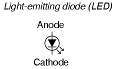
This notation of having two small arrows pointing away from the device is common to the schematic symbols of all light-emitting semiconductor devices. Conversely, if a device is light-activated (meaning that incoming light stimulates it), then the symbol will have two small arrows pointing toward it. It is interesting to note, though, that LEDs are capable of acting as light-sensing devices: they will generate a small voltage when exposed to light, much like a solar cell on a small scale. This property can be gainfully applied in a variety of light-sensing circuits.
Because LEDs are made of different chemical substances than normal rectifying diodes, their forward voltage drops will be different. Typically, LEDs have much larger forward voltage drops than rectifying diodes, anywhere from about 1.6 volts to over 3 volts, depending on the color. Typical operating current for a standard-sized LED is around 20 mA. When operating an LED from a DC voltage source greater than the LED's forward voltage, a series-connected "dropping" resistor must be included to prevent full source voltage from damaging the LED. Consider this example circuit:

With the LED dropping 1.6 volts, there will be 4.4 volts dropped across the resistor. Sizing the resistor for an LED current of 20 mA is as simple as taking its voltage drop (4.4 volts) and dividing by circuit current (20 mA), in accordance with Ohm's Law (R=E/I). This gives us a figure of 220 Ω. Calculating power dissipation for this resistor, we take its voltage drop and multiply by its current (P=IE), and end up with 88 mW, well within the rating of a 1/8 watt resistor. Higher battery voltages will require larger-value dropping resistors, and possibly higher-power rating resistors as well. Consider this example for a supply voltage of 24 volts:

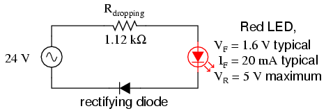
Here, the dropping resistor must be increased to a size of 1.12 kΩ in order to drop 22.4 volts at 20 mA so that the LED still receives only 1.6 volts. This also makes for a higher resistor power dissipation: 448 mW, nearly one-half a watt of power! Obviously, a resistor rated for 1/8 watt power dissipation or even 1/4 watt dissipation will overheat if used here.
Dropping resistor values need not be precise for LED circuits. Suppose we were to use a 1 kΩ resistor instead of a 1.12 kΩ resistor in the circuit shown above. The result would be a slightly greater circuit current and LED voltage drop, resulting in a brighter light from the LED and slightly reduced service life. A dropping resistor with too much resistance (say, 1.5 kΩ instead of 1.12 kΩ) will result in less circuit current, less LED voltage, and a dimmer light. LEDs are quite tolerant of variation in applied power, so you need not strive for perfection in sizing the dropping resistor.
Also because of their unique chemical makeup, LEDs have much, much lower peak-inverse voltage (PIV) ratings than ordinary rectifying diodes. A typical LED might only be rated at 5 volts in reverse-bias mode. Therefore, when using alternating current to power an LED, you should connect a protective rectifying diode in series with the LED to prevent reverse breakdown every other half-cycle:
As lamps, LEDs are superior to incandescent bulbs in many ways. First and foremost is efficiency: LEDs output far more light power per watt than an incandescent lamp. This is a significant advantage if the circuit in question is battery-powered, efficiency translating to longer battery life. Second is the fact that LEDs are far more reliable, having a much greater service life than an incandescent lamp. This advantage is primarily due to the fact that LEDs are "cold" devices: they operate at much cooler temperatures than an incandescent lamp with a white-hot metal filament, susceptible to breakage from mechanical and thermal shock. Third is the high speed at which LEDs may be turned on and off. This advantage is also due to the "cold" operation of LEDs: they don't have to overcome thermal inertia in transitioning from off to on or vice versa. For this reason, LEDs are used to transmit digital (on/off) information as pulses of light, conducted in empty space or through fiber-optic cable, at very high rates of speed (millions of pulses per second).
One major disadvantage of using LEDs as sources of illumination is their monochromatic (single-color) emission. No one wants to read a book under the light of a red, green, or blue LED. However, if used in combination, LED colors may be mixed for a more broad-spectrum glow.
Laser diodes
The laser diode is a further development upon the regular light-emitting diode, or LED. The term "laser" itself is actually an acronym, despite the fact it's often written in lower-case letters. "Laser" stands for Light Amplification by Stimulated Emission of Radiation, and refers to another strange quantum process whereby characteristic light emitted by electrons transitioning from high-level to low-level energy states in a material stimulate other electrons in a substance to make similar "jumps," the result being a synchronized output of light from the material. This synchronization extends to the actual phase of the emitted light, so that all light waves emitted from a "lasing" material are not just the same frequency (color), but also the same phase as each other, so that they reinforce one another and are able to travel in a very tightly-confined, nondispersing beam. This is why laser light stays so remarkably focused over long distances: each and every light wave coming from the laser is in step with each other:
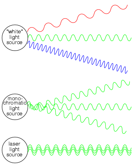
Incandescent lamps produce "white" (mixed-frequency, or mixed-color) light. Regular LEDs produce monochromatic light: same frequency (color), but different phases, resulting in similar beam dispersion. Laser LEDs produce coherent light: light that is both monochromatic (single-color) and monophasic (single-phase), resulting in precise beam confinement.
Laser light finds wide application in the modern world: everything from surveying, where a straight and nondispersing light beam is very useful for precise sighting of measurement markers, to the reading and writing of optical disks, where only the narrowness of a focused laser beam is able to resolve the microscopic "pits" in the disk's surface comprising the binary 1's and 0's of digital information.
Some laser diodes require special high-power "pulsing" circuits to deliver large quantities of voltage and current in short bursts. Other laser diodes may be operated continuously at lower power. In the latter case, laser action occurs only within a certain range of diode current, necessitating some form of current-regulator circuit. As laser diodes age, their power requirements may change (more current required for less output power), but it should be remembered that low-power laser diodes, like LEDs, are fairly long-lived devices, with typical service lives in the tens of thousands of hours.
Photodiodes
Varactor diodes
Constant-current diodes
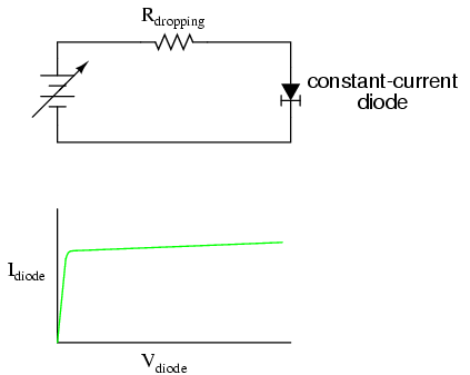
A constant-current diode, also known as a current-limiting diode, or current-regulating diode, does exactly what its name implies: it regulates current through it to some maximum level. If you try to force more current through a constant-current diode than its current-regulation point, it simply "fights back" by dropping more voltage. If we were to build the following circuit and plot diode current over diode current, we'd get a graph that rises normally at first and then levels off at the current regulation point:
One interesting application for a constant-current diode is to automatically limit current through an LED or laser diode over a wide range of power supply voltages, like this:
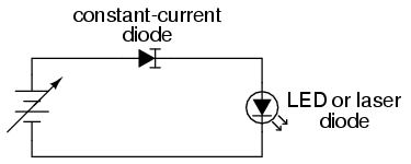
Of course, the constant-current diode's regulation point should be chosen to match the LED or laser diode's optimum forward current. This is especially important for the laser diode, not so much for the LED, as regular LEDs tend to be more tolerant of forward current variations.
Another application is in the charging of small secondary-cell batteries, where a constant charging current leads to very predictable charging times. Of course, large secondary-cell battery banks might also benefit from constant-current charging, but constant-current diodes tend to be very small devices, limited to regulating currents in the milliamp range.
Other diode technologies
Contributors
Contributors to this chapter are listed in chronological order of their contributions, from most recent to first. See Appendix 2 (Contributor List) for dates and contact information.
Jered Wierzbicki (December 2002): Pointed out error in diode equation -- Boltzmann's constant shown incorrectly.
Lessons In Electric Circuits copyright (C) 2000-2006 Tony R. Kuphaldt, under the terms and conditions of the semi_a3Design Science License.
Previous Contents
 Next
Next
