Lessons In Electric Circuits -- Volume III (Semiconductors) - Chapter 4
Previous Contents
 Next
Next
Lessons In Electric Circuits -- Volume III
Chapter 4
BIPOLAR JUNCTION TRANSISTORS
- Introduction
- The transistor as a switch
- Meter check of a transistor
- Active mode operation
- The common-emitter amplifier
- The common-collector amplifier
- The common-base amplifier
- Biasing techniques
- Input and output coupling
- Feedback
- Amplifier impedances
- Current mirrors
- Transistor ratings and packages
- BJT quirks
*** INCOMPLETE ***
Introduction
The invention of the bipolar transistor in 1948 ushered in a revolution in electronics. Technical feats previously requiring relatively large, mechanically fragile, power-hungry vacuum tubes were suddenly achievable with tiny, mechanically rugged, power-thrifty specks of crystalline silicon. This revolution made possible the design and manufacture of lightweight, inexpensive electronic devices that we now take for granted. Understanding how transistors function is of paramount importance to anyone interested in understanding modern electronics.
My intent here is to focus as exclusively as possible on the practical function and application of bipolar transistors, rather than to explore the quantum world of semiconductor theory. Discussions of holes and electrons are better left to another chapter in my opinion. Here I want to explore how to use these components, not analyze their intimate internal details. I don't mean to downplay the importance of understanding semiconductor physics, but sometimes an intense focus on solid-state physics detracts from understanding these devices' functions on a component level. In taking this approach, however, I assume that the reader possesses a certain minimum knowledge of semiconductors: the difference between "P" and "N" doped semiconductors, the functional characteristics of a PN (diode) junction, and the meanings of the terms "reverse biased" and "forward biased." If these concepts are unclear to you, it is best to refer to earlier chapters in this book before proceeding with this one.
A bipolar transistor consists of a three-layer "sandwich" of doped (extrinsic) semiconductor materials, either P-N-P or N-P-N. Each layer forming the transistor has a specific name, and each layer is provided with a wire contact for connection to a circuit. Shown here are schematic symbols and physical diagrams of these two transistor types:
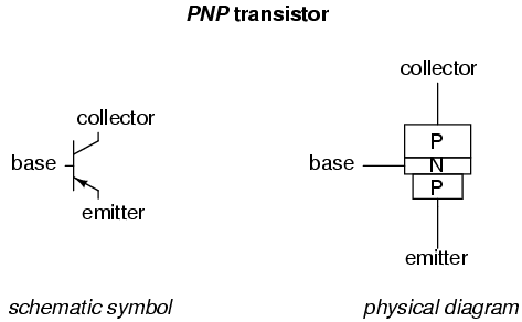
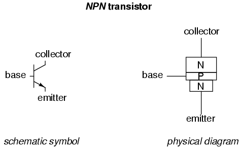
The only functional difference between a PNP transistor and an NPN transistor is the proper biasing (polarity) of the junctions when operating. For any given state of operation, the current directions and voltage polarities for each type of transistor are exactly opposite each other.
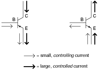
Bipolar transistors work as current-controlled current regulators. In other words, they restrict the amount of current that can go through them according to a smaller, controlling current. The main current that is controlled goes from collector to emitter, or from emitter to collector, depending on the type of transistor it is (PNP or NPN, respectively). The small current that controls the main current goes from base to emitter, or from emitter to base, once again depending on the type of transistor it is (PNP or NPN, respectively). According to the confusing standards of semiconductor symbology, the arrow always points against the direction of electron flow:
Bipolar transistors are called bipolar because the main flow of electrons through them takes place in two types of semiconductor material: P and N, as the main current goes from emitter to collector (or vice versa). In other words, two types of charge carriers -- electrons and holes -- comprise this main current through the transistor.
As you can see, the controlling current and the controlled current always mesh together through the emitter wire, and their electrons always flow against the direction of the transistor's arrow. This is the first and foremost rule in the use of transistors: all currents must be going in the proper directions for the device to work as a current regulator. The small, controlling current is usually referred to simply as the base current because it is the only current that goes through the base wire of the transistor. Conversely, the large, controlled current is referred to as the collector current because it is the only current that goes through the collector wire. The emitter current is the sum of the base and collector currents, in compliance with Kirchhoff's Current Law.
If there is no current through the base of the transistor, it shuts off like an open switch and prevents current through the collector. If there is a base current, then the transistor turns on like a closed switch and allows a proportional amount of current through the collector. Collector current is primarily limited by the base current, regardless of the amount of voltage available to push it. The next section will explore in more detail the use of bipolar transistors as switching elements.
- REVIEW:
- Bipolar transistors are so named because the controlled current must go through two types of semiconductor material: P and N. The current consists of both electron and hole flow, in different parts of the transistor.
- Bipolar transistors consist of either a P-N-P or an N-P-N semiconductor "sandwich" structure.
- The three leads of a bipolar transistor are called the Emitter, Base, and Collector.
- Transistors function as current regulators by allowing a small current to control a larger current. The amount of current allowed between collector and emitter is primarily determined by the amount of current moving between base and emitter.
- In order for a transistor to properly function as a current regulator, the controlling (base) current and the controlled (collector) currents must be going in the proper directions: meshing additively at the emitter and going against the emitter arrow symbol.
The transistor as a switch
Because a transistor's collector current is proportionally limited by its base current, it can be used as a sort of current-controlled switch. A relatively small flow of electrons sent through the base of the transistor has the ability to exert control over a much larger flow of electrons through the collector.
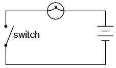
Suppose we had a lamp that we wanted to turn on and off by means of a switch. Such a circuit would be extremely simple:
For the sake of illustration, let's insert a transistor in place of the switch to show how it can control the flow of electrons through the lamp. Remember that the controlled current through a transistor must go between collector and emitter. Since it's the current through the lamp that we want to control, we must position the collector and emitter of our transistor where the two contacts of the switch are now. We must also make sure that the lamp's current will move against the direction of the emitter arrow symbol to ensure that the transistor's junction bias will be correct:
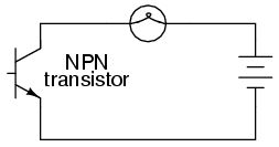
In this example I happened to choose an NPN transistor. A PNP transistor could also have been chosen for the job, and its application would look like this:
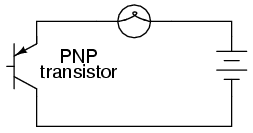
The choice between NPN and PNP is really arbitrary. All that matters is that the proper current directions are maintained for the sake of correct junction biasing (electron flow going against the transistor symbol's arrow).
Going back to the NPN transistor in our example circuit, we are faced with the need to add something more so that we can have base current. Without a connection to the base wire of the transistor, base current will be zero, and the transistor cannot turn on, resulting in a lamp that is always off. Remember that for an NPN transistor, base current must consist of electrons flowing from emitter to base (against the emitter arrow symbol, just like the lamp current). Perhaps the simplest thing to do would be to connect a switch between the base and collector wires of the transistor like this:
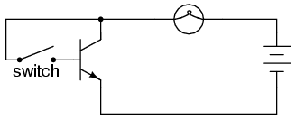
If the switch is open, the base wire of the transistor will be left "floating" (not connected to anything) and there will be no current through it. In this state, the transistor is said to be cutoff. If the switch is closed, however, electrons will be able to flow from the emitter through to the base of the transistor, through the switch and up to the left side of the lamp, back to the positive side of the battery. This base current will enable a much larger flow of electrons from the emitter through to the collector, thus lighting up the lamp. In this state of maximum circuit current, the transistor is said to be saturated.
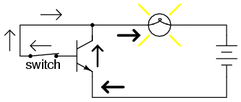
Of course, it may seem pointless to use a transistor in this capacity to control the lamp. After all, we're still using a switch in the circuit, aren't we? If we're still using a switch to control the lamp -- if only indirectly -- then what's the point of having a transistor to control the current? Why not just go back to our original circuit and use the switch directly to control the lamp current?
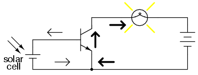
There are a couple of points to be made here, actually. First is the fact that when used in this manner, the switch contacts need only handle what little base current is necessary to turn the transistor on, while the transistor itself handles the majority of the lamp's current. This may be an important advantage if the switch has a low current rating: a small switch may be used to control a relatively high-current load. Perhaps more importantly, though, is the fact that the current-controlling behavior of the transistor enables us to use something completely different to turn the lamp on or off. Consider this example, where a solar cell is used to control the transistor, which in turn controls the lamp:
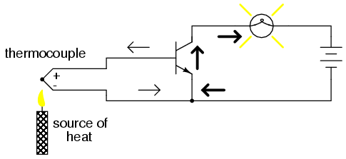
Or, we could use a thermocouple to provide the necessary base current to turn the transistor on:
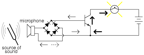
Even a microphone of sufficient voltage and current output could be used to turn the transistor on, provided its output is rectified from AC to DC so that the emitter-base PN junction within the transistor will always be forward-biased:
The point should be quite apparent by now: any sufficient source of DC current may be used to turn the transistor on, and that source of current need only be a fraction of the amount of current needed to energize the lamp. Here we see the transistor functioning not only as a switch, but as a true amplifier: using a relatively low-power signal to control a relatively large amount of power. Please note that the actual power for lighting up the lamp comes from the battery to the right of the schematic. It is not as though the small signal current from the solar cell, thermocouple, or microphone is being magically transformed into a greater amount of power. Rather, those small power sources are simply controlling the battery's power to light up the lamp.
- REVIEW:
- Transistors may be used as switching elements to control DC power to a load. The switched (controlled) current goes between emitter and collector, while the controlling current goes between emitter and base.
- When a transistor has zero current through it, it is said to be in a state of cutoff (fully nonconducting).
- When a transistor has maximum current through it, it is said to be in a state of saturation (fully conducting).
Meter check of a transistor
Bipolar transistors are constructed of a three-layer semiconductor "sandwich," either PNP or NPN. As such, they register as two diodes connected back-to-back when tested with a multimeter's "resistance" or "diode check" functions:
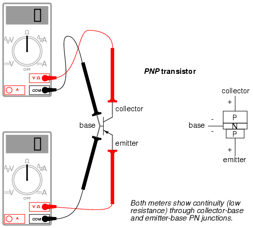
Here I'm assuming the use of a multimeter with only a single continuity range (resistance) function to check the PN junctions. Some multimeters are equipped with two separate continuity check functions: resistance and "diode check," each with its own purpose. If your meter has a designated "diode check" function, use that rather than the "resistance" range, and the meter will display the actual forward voltage of the PN junction and not just whether or not it conducts current.
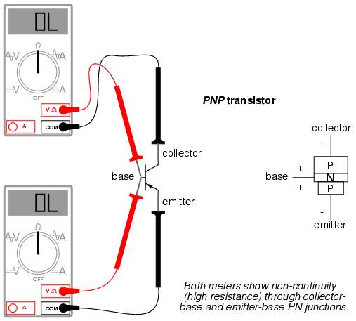
Meter readings will be exactly opposite, of course, for an NPN transistor, with both PN junctions facing the other way. If a multimeter with a "diode check" function is used in this test, it will be found that the emitter-base junction possesses a slightly greater forward voltage drop than the collector-base junction. This forward voltage difference is due to the disparity in doping concentration between the emitter and collector regions of the transistor: the emitter is a much more heavily doped piece of semiconductor material than the collector, causing its junction with the base to produce a higher forward voltage drop.
Knowing this, it becomes possible to determine which wire is which on an unmarked transistor. This is important because transistor packaging, unfortunately, is not standardized. All bipolar transistors have three wires, of course, but the positions of the three wires on the actual physical package are not arranged in any universal, standardized order.
Suppose a technician finds a bipolar transistor and proceeds to measure continuity with a multimeter set in the "diode check" mode. Measuring between pairs of wires and recording the values displayed by the meter, the technician obtains the following data:
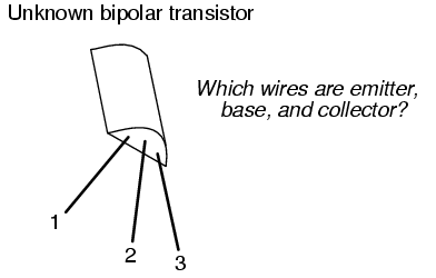
- Meter touching wire 1 (+) and 2 (-): "OL"
- Meter touching wire 1 (-) and 2 (+): "OL"
- Meter touching wire 1 (+) and 3 (-): 0.655 volts
- Meter touching wire 1 (-) and 3 (+): "OL"
- Meter touching wire 2 (+) and 3 (-): 0.621 volts
- Meter touching wire 2 (-) and 3 (+): "OL"
The only combinations of test points giving conducting meter readings are wires 1 and 3 (red test lead on 1 and black test lead on 3), and wires 2 and 3 (red test lead on 2 and black test lead on 3). These two readings must indicate forward biasing of the emitter-to-base junction (0.655 volts) and the collector-to-base junction (0.621 volts).
Now we look for the one wire common to both sets of conductive readings. It must be the base connection of the transistor, because the base is the only layer of the three-layer device common to both sets of PN junctions (emitter-base and collector-base). In this example, that wire is number 3, being common to both the 1-3 and the 2-3 test point combinations. In both those sets of meter readings, the black (-) meter test lead was touching wire 3, which tells us that the base of this transistor is made of N-type semiconductor material (black = negative). Thus, the transistor is an PNP type with base on wire 3, emitter on wire 1 and collector on wire 2:
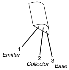
Please note that the base wire in this example is not the middle lead of the transistor, as one might expect from the three-layer "sandwich" model of a bipolar transistor. This is quite often the case, and tends to confuse new students of electronics. The only way to be sure which lead is which is by a meter check, or by referencing the manufacturer's "data sheet" documentation on that particular part number of transistor.
Knowing that a bipolar transistor behaves as two back-to-back diodes when tested with a conductivity meter is helpful for identifying an unknown transistor purely by meter readings. It is also helpful for a quick functional check of the transistor. If the technician were to measure continuity in any more than two or any less than two of the six test lead combinations, he or she would immediately know that the transistor was defective (or else that it wasn't a bipolar transistor but rather something else -- a distinct possibility if no part numbers can be referenced for sure identification!). However, the "two diode" model of the transistor fails to explain how or why it acts as an amplifying device.
To better illustrate this paradox, let's examine one of the transistor switch circuits using the physical diagram rather than the schematic symbol to represent the transistor. This way the two PN junctions will be easier to see:
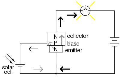
A grey-colored diagonal arrow shows the direction of electron flow through the emitter-base junction. This part makes sense, since the electrons are flowing from the N-type emitter to the P-type base: the junction is obviously forward-biased. However, the base-collector junction is another matter entirely. Notice how the grey-colored thick arrow is pointing in the direction of electron flow (upwards) from base to collector. With the base made of P-type material and the collector of N-type material, this direction of electron flow is clearly backwards to the direction normally associated with a PN junction! A normal PN junction wouldn't permit this "backward" direction of flow, at least not without offering significant opposition. However, when the transistor is saturated, there is very little opposition to electrons all the way from emitter to collector, as evidenced by the lamp's illumination!
Clearly then, something is going on here that defies the simple "two-diode" explanatory model of the bipolar transistor. When I was first learning about transistor operation, I tried to construct my own transistor from two back-to-back diodes, like this:
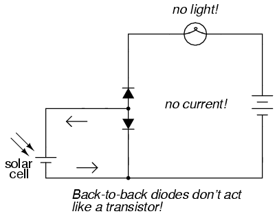
My circuit didn't work, and I was mystified. However useful the "two diode" description of a transistor might be for testing purposes, it doesn't explain how a transistor can behave as a controlled switch.
What happens in a transistor is this: the reverse bias of the base-collector junction prevents collector current when the transistor is in cutoff mode (that is, when there is no base current). However, when the base-emitter junction is forward biased by the controlling signal, the normally-blocking action of the base-collector junction is overridden and current is permitted through the collector, despite the fact that electrons are going the "wrong way" through that PN junction. This action is dependent on the quantum physics of semiconductor junctions, and can only take place when the two junctions are properly spaced and the doping concentrations of the three layers are properly proportioned. Two diodes wired in series fail to meet these criteria, and so the top diode can never "turn on" when it is reversed biased, no matter how much current goes through the bottom diode in the base wire loop.
That doping concentrations play a crucial part in the special abilities of the transistor is further evidenced by the fact that collector and emitter are not interchangeable. If the transistor is merely viewed as two back-to-back PN junctions, or merely as a plain N-P-N or P-N-P sandwich of materials, it may seem as though either end of the transistor could serve as collector or emitter. This, however, is not true. If connected "backwards" in a circuit, a base-collector current will fail to control current between collector and emitter. Despite the fact that both the emitter and collector layers of a bipolar transistor are of the same doping type (either N or P), they are definitely not identical!
So, current through the emitter-base junction allows current through the reverse-biased base-collector junction. The action of base current can be thought of as "opening a gate" for current through the collector. More specifically, any given amount of emitter-to-base current permits a limited amount of base-to-collector current. For every electron that passes through the emitter-base junction and on through the base wire, there is allowed a certain, restricted number of electrons to pass through the base-collector junction and no more.
In the next section, this current-limiting behavior of the transistor will be investigated in more detail.
- REVIEW:
- Tested with a multimeter in the "resistance" or "diode check" modes, a transistor behaves like two back-to-back PN (diode) junctions.
- The emitter-base PN junction has a slightly greater forward voltage drop than the collector-base PN junction, due to more concentrated doping of the emitter semiconductor layer.
- The reverse-biased base-collector junction normally blocks any current from going through the transistor between emitter and collector. However, that junction begins to conduct if current is drawn through the base wire. Base current can be thought of as "opening a gate" for a certain, limited amount of current through the collector.
Active mode operation
When a transistor is in the fully-off state (like an open switch), it is said to be cutoff. Conversely, when it is fully conductive between emitter and collector (passing as much current through the collector as the collector power supply and load will allow), it is said to be saturated. These are the two modes of operation explored thus far in using the transistor as a switch.
However, bipolar transistors don't have to be restricted to these two extreme modes of operation. As we learned in the previous section, base current "opens a gate" for a limited amount of current through the collector. If this limit for the controlled current is greater than zero but less than the maximum allowed by the power supply and load circuit, the transistor will "throttle" the collector current in a mode somewhere between cutoff and saturation. This mode of operation is called the active mode.
An automotive analogy for transistor operation is as follows: cutoff is the condition where there is no motive force generated by the mechanical parts of the car to make it move. In cutoff mode, the brake is engaged (zero base current), preventing motion (collector current). Active mode is when the automobile is cruising at a constant, controlled speed (constant, controlled collector current) as dictated by the driver. Saturation is when the automobile is driving up a steep hill that prevents it from going as fast as the driver would wish. In other words, a "saturated" automobile is one where the accelerator pedal is pushed all the way down (base current calling for more collector current than can be provided by the power supply/load circuit).
I'll set up a circuit for SPICE simulation to demonstrate what happens when a transistor is in its active mode of operation:
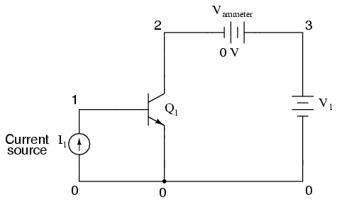
"Q" is the standard letter designation for a transistor in a schematic diagram, just as "R" is for resistor and "C" is for capacitor. In this circuit, we have an NPN transistor powered by a battery (V1) and controlled by current through a current source (I1). A current source is a device that outputs a specific amount of current, generating as much or as little voltage as necessary across its terminals to ensure that exact amount of current through it. Current sources are notoriously difficult to find in nature (unlike voltage sources, which by contrast attempt to maintain a constant voltage, outputting as much or as little current in the fulfillment of that task), but can be simulated with a small collection of electronic components. As we are about to see, transistors themselves tend to mimic the constant-current behavior of a current source in their ability to regulate current at a fixed value.
In the SPICE simulation, I'll set the current source at a constant value of 20 µA, then vary the voltage source (V1) over a range of 0 to 2 volts and monitor how much current goes through it. The "dummy" battery (Vammeter) with its output of 0 volts serves merely to provide SPICE with a circuit element for current measurement.
bipolar transistor simulation i1 0 1 dc 20u q1 2 1 0 mod1 vammeter 3 2 dc 0 v1 3 0 dc .model mod1 npn .dc v1 0 2 0.05 .plot dc i(vammeter) .end
type npn is 1.00E-16bf 100.000nf 1.000br 1.000nr 1.000
We can perform another computer analysis of this circuit, only this time instructing SPICE to analyze it from an AC point of view, giving us peak voltage figures for input and output instead of a time-based plot of the waveforms:
common-emitter amplifier vinput 1 5 ac 1.5 vbias 5 0 dc 2.3r1 1 2 1k q1 3 2 0 mod1 rspkr 3 4 30 v1 4 0 dc 15 .model mod1 npn .ac lin 1 2000 2000 .print ac v(1,0) v(4,3) .end
freq v(1) v(4,3) 2.000E+03 1.500E+00 4.418E+00
Peak voltage measurements of input and output show an input of 1.5 volts and an output of 4.418 volts. This gives us a voltage gain ratio of 2.9453 (4.418 V / 1.5 V), or 9.3827 dB.
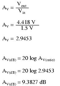
Because the current gain of the common-emitter amplifier is fixed by β, and since the input and output voltages will be equal to the input and output currents multiplied by their respective resistors, we can derive an equation for approximate voltage gain:
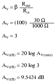
As you can see, the predicted results for voltage gain are quite close to the simulated results. With perfectly linear transistor behavior, the two sets of figures would exactly match. SPICE does a reasonable job of accounting for the many "quirks" of bipolar transistor function in its analysis, hence the slight mismatch in voltage gain based on SPICE's output.
These voltage gains remain the same regardless of where we measure output voltage in the circuit: across collector and emitter, or across the series load resistor as we did in the last analysis. The amount of output voltage change for any given amount of input voltage will remain the same. Consider the two following SPICE analyses as proof of this. The first simulation is time-based, to provide a plot of input and output voltages. You will notice that the two signals are 180o out of phase with each other. The second simulation is an AC analysis, to provide simple, peak voltage readings for input and output:
common-emitter amplifier vinput 1 5 sin (0 1.5 2000 0 0) vbias 5 0 dc 2.3r1 1 2 1k q1 3 2 0 mod1 rspkr 3 4 30 v1 4 0 dc 15 .model mod1 npn .tran 0.02m 0.74m .plot tran v(1,0) v(3,0).end
