Lessons In Electric Circuits -- Volume III (Semiconductors) - Chapter 5
Previous Contents
 Next
Next
Lessons In Electric Circuits -- Volume III
Chapter 5
JUNCTION FIELD-EFFECT TRANSISTORS
- Introduction
- The transistor as a switch
- Meter check of a transistor
- Active-mode operation
- The common-source amplifier -- PENDING
- The common-drain amplifier -- PENDING
- The common-gate amplifier -- PENDING
- Biasing techniques -- PENDING
- Transistor ratings and packages -- PENDING
- JFET quirks -- PENDING
*** INCOMPLETE ***
Introduction
A transistor is a linear semiconductor device that controls current with the application of a lower-power electrical signal. Transistors may be roughly grouped into two major divisions: bipolar and field-effect. In the last chapter we studied bipolar transistors, which utilize a small current to control a large current. In this chapter, we'll introduce the general concept of the field-effect transistor -- a device utilizing a small voltage to control current -- and then focus on one particular type: the junction field-effect transistor. In the next chapter we'll explore another type of field-effect transistor, the insulated gate variety.
All field-effect transistors are unipolar rather than bipolar devices. That is, the main current through them is comprised either of electrons through an N-type semiconductor or holes through a P-type semiconductor. This becomes more evident when a physical diagram of the device is seen:
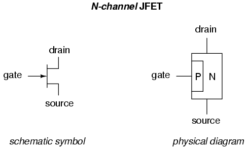
In a junction field-effect transistor, or JFET, the controlled current passes from source to drain, or from drain to source as the case may be. The controlling voltage is applied between the gate and source. Note how the current does not have to cross through a PN junction on its way between source and drain: the path (called a channel) is an uninterrupted block of semiconductor material. In the image just shown, this channel is an N-type semiconductor. P-type channel JFETs are also manufactured:
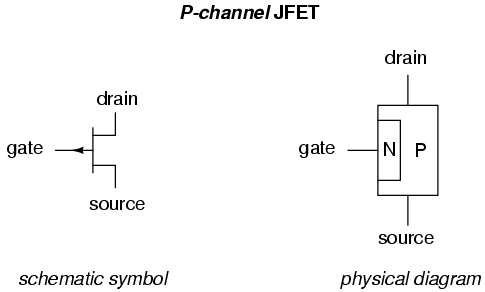
Generally, N-channel JFETs are more commonly used than P-channel. The reasons for this have to do with obscure details of semiconductor theory, which I'd rather not discuss in this chapter. As with bipolar transistors, I believe the best way to introduce field-effect transistor usage is to avoid theory whenever possible and concentrate instead on operational characteristics. The only practical difference between N- and P-channel JFETs you need to concern yourself with now is biasing of the PN junction formed between the gate material and the channel.
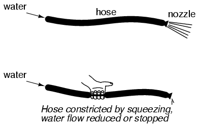
With no voltage applied between gate and source, the channel is a wide-open path for electrons to flow. However, if a voltage is applied between gate and source of such polarity that it reverse-biases the PN junction, the flow between source and drain connections becomes limited, or regulated, just as it was for bipolar transistors with a set amount of base current. Maximum gate-source voltage "pinches off" all current through source and drain, thus forcing the JFET into cutoff mode. This behavior is due to the depletion region of the PN junction expanding under the influence of a reverse-bias voltage, eventually occupying the entire width of the channel if the voltage is great enough. This action may be likened to reducing the flow of a liquid through a flexible hose by squeezing it: with enough force, the hose will be constricted enough to completely block the flow.
Note how this operational behavior is exactly opposite of the bipolar junction transistor. Bipolar transistors are normally-off devices: no current through the base, no current through the collector or the emitter. JFETs, on the other hand, are normally-on devices: no voltage applied to the gate allows maximum current through the source and drain. Also take note that the amount of current allowed through a JFET is determined by a voltage signal rather than a current signal as with bipolar transistors. In fact, with the gate-source PN junction reverse-biased, there should be nearly zero current through the gate connection. For this reason, we classify the JFET as a voltage-controlled device, and the bipolar transistor as a current-controlled device.
If the gate-source PN junction is forward-biased with a small voltage, the JFET channel will "open" a little more to allow greater currents through. However, the PN junction of a JFET is not built to handle any substantial current itself, and thus it is not recommended to forward-bias the junction under any circumstances.
This is a very condensed overview of JFET operation. In the next section, we'll explore the use of the JFET as a switching device.
The transistor as a switch
Like its bipolar cousin, the field-effect transistor may be used as an on/off switch controlling electrical power to a load. Let's begin our investigation of the JFET as a switch with our familiar switch/lamp circuit:
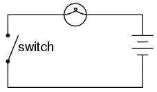
Remembering that the controlled current in a JFET flows between source and drain, we substitute the source and drain connections of a JFET for the two ends of the switch in the above circuit:

If you haven't noticed by now, the source and drain connections on a JFET look identical on the schematic symbol. Unlike the bipolar junction transistor where the emitter is clearly distinguished from the collector by the arrowhead, a JFET's source and drain lines both run perpendicular into the bar representing the semiconductor channel. This is no accident, as the source and drain lines of a JFET are often interchangeable in practice! In other words, JFETs are usually able to handle channel current in either direction, from source to drain or from drain to source.
Now all we need in the circuit is a way to control the JFET's conduction. With zero applied voltage between gate and source, the JFET's channel will be "open," allowing full current to the lamp. In order to turn the lamp off, we will need to connect another source of DC voltage between the gate and source connections of the JFET like this:
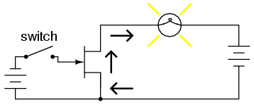
Closing this switch will "pinch off" the JFET's channel, thus forcing it into cutoff and turning the lamp off:
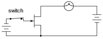
Note that there is no current going through the gate. As a reverse-biased PN junction, it firmly opposes the flow of any electrons through it. As a voltage-controlled device, the JFET requires negligible input current. This is an advantageous trait of the JFET over the bipolar transistor: there is virtually zero power required of the controlling signal.
Opening the control switch again should disconnect the reverse-biasing DC voltage from the gate, thus allowing the transistor to turn back on. Ideally, anyway, this is how it works. In practice this may not work at all:

Why is this? Why doesn't the JFET's channel open up again and allow lamp current through like it did before with no voltage applied between gate and source? The answer lies in the operation of the reverse-biased gate-source junction. The depletion region within that junction acts as an insulating barrier separating gate from source. As such, it possesses a certain amount of capacitance capable of storing an electric charge potential. After this junction has been forcibly reverse-biased by the application of an external voltage, it will tend to hold that reverse-biasing voltage as a stored charge even after the source of that voltage has been disconnected. What is needed to turn the JFET on again is to bleed off that stored charge between the gate and source through a resistor:
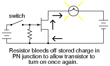
This resistor's value is not very important. The capacitance of the JFET's gate-source junction is very small, and so even a rather high-value bleed resistor creates a fast RC time constant, allowing the transistor to resume conduction with little delay once the switch is opened.
Like the bipolar transistor, it matters little where or what the controlling voltage comes from. We could use a solar cell, thermocouple, or any other sort of voltage-generating device to supply the voltage controlling the JFET's conduction. All that is required of a voltage source for JFET switch operation is sufficient voltage to achieve pinch-off of the JFET channel. This level is usually in the realm of a few volts DC, and is termed the pinch-off or cutoff voltage. The exact pinch-off voltage for any given JFET is a function of its unique design, and is not a universal figure like 0.7 volts is for a silicon BJT's base-emitter junction voltage.
- REVIEW:
- Field-effect transistors control the current between source and drain connections by a voltage applied between the gate and source. In a junction field-effect transistor (JFET), there is a PN junction between the gate and source which is normally reverse-biased for control of source-drain current.
- JFETs are normally-on (normally-saturated) devices. The application of a reverse-biasing voltage between gate and source causes the depletion region of that junction to expand, thereby "pinching off" the channel between source and drain through which the controlled current travels.
- It may be necessary to attach a "bleed-off" resistor between gate and source to discharge the stored charge built up across the junction's natural capacitance when the controlling voltage is removed. Otherwise, a charge may remain to keep the JFET in cutoff mode even after the voltage source has been disconnected.
Meter check of a transistor
Testing a JFET with a multimeter might seem to be a relatively easy task, seeing as how it has only one PN junction to test: either measured between gate and source, or between gate and drain.


Testing continuity through the drain-source channel is another matter, though. Remember from the last section how a stored charge across the capacitance of the gate-channel PN junction could hold the JFET in a pinched-off state without any external voltage being applied across it? This can occur even when you're holding the JFET in your hand to test it! Consequently, any meter reading of continuity through that channel will be unpredictable, since you don't necessarily know if a charge is being stored by the gate-channel junction. Of course, if you know beforehand which terminals on the device are the gate, source, and drain, you may connect a jumper wire between gate and source to eliminate any stored charge and then proceed to test source-drain continuity with no problem. However, if you don't know which terminals are which, the unpredictability of the source-drain connection may confuse your determination of terminal identity.
A good strategy to follow when testing a JFET is to insert the pins of the transistor into anti-static foam (the material used to ship and store static-sensitive electronic components) just prior to testing. The conductivity of the foam will make a resistive connection between all terminals of the transistor when it is inserted. This connection will ensure that all residual voltage built up across the gate-channel PN junction will be neutralized, thus "opening up" the channel for an accurate meter test of source-to-drain continuity.
Since the JFET channel is a single, uninterrupted piece of semiconductor material, there is usually no difference between the source and drain terminals. A resistance check from source to drain should yield the same value as a check from drain to source. This resistance should be relatively low (a few hundred ohms at most) when the gate-source PN junction voltage is zero. By applying a reverse-bias voltage between gate and source, pinch-off of the channel should be apparent by an increased resistance reading on the meter.
Active-mode operation
JFETs, like bipolar transistors, are able to "throttle" current in a mode between cutoff and saturation called the active mode. To better understand JFET operation, let's set up a SPICE simulation similar to the one used to explore basic bipolar transistor function:
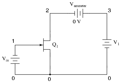
jfet simulation vin 0 1 dc 1 j1 2 1 0 mod1 vammeter 3 2 dc 0 v1 3 0 dc .model mod1 njf .dc v1 0 2 0.05 .plot dc i(vammeter) .end
Note that the transistor labeled "Q1" in the schematic is represented in the SPICE netlist as j1. Although all transistor types are commonly referred to as "Q" devices in circuit schematics -- just as resistors are referred to by "R" designations, and capacitors by "C" -- SPICE needs to be told what type of transistor this is by means of a different letter designation: q for bipolar junction transistors, and j for junction field-effect transistors.
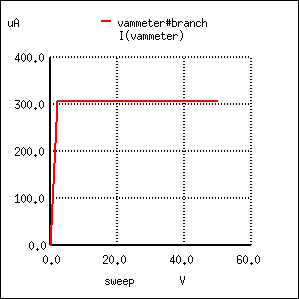
With the gate-source voltage set to 0.25 volts, one-half what it was before, the drain current is 306.3 µA. Although this is still an increase over the 225 µA from the prior simulation, it isn't proportional to the change of the controlling voltage.
To obtain a better understanding of what is going on here, we should run a different kind of simulation: one that keeps the power supply voltage constant and instead varies the controlling (voltage) signal. When this kind of simulation was run on a BJT, the result was a straight-line graph, showing how the input current / output current relationship of a BJT is linear. Let's see what kind of relationship a JFET exhibits:
jfet simulation vin 0 1 dc j1 2 1 0 mod1 vammeter 3 2 dc 0 v1 3 0 dc 25 .model mod1 njf .dc vin 0 2 0.1 .plot dc i(vammeter) .end
- REVIEW:
Lessons In Electric Circuits copyright (C) 2000-2006 Tony R. Kuphaldt, under the terms and conditions of the semi_a3Design Science License.
Previous Contents
 Next
Next
